What is the definition of thin? That depends on who you ask and what their capabilities are. At Sydor Optics, our definition of thin wafer processing is around 500 microns, but we like to work on the ultra-thin side. We consider ultra-thin at 100-200 microns in overall thickness. To put this thickness into context, the average human hair is ~100 microns thick. That is really thin, especially for glass!
We can process glass in the thickness range of 100-200 microns in either a single-side or double-side process. There are advantages to both processes, but we have optimized each process to achieve the specifications that our customers are requesting. Here are some important factors to consider when processing thin substrates.
- The condition of the incoming blank is critical to the survival of the final substrate. It is vital to ensure that the edges have no significant chips or fractures that would cause the substrate to have a fatal issue during processing.
- Glass does have elasticity so the way the surfaces are prepared is also extremely important. If the surfaces have significant waviness, this will translate to the final part, especially during the double-side process.
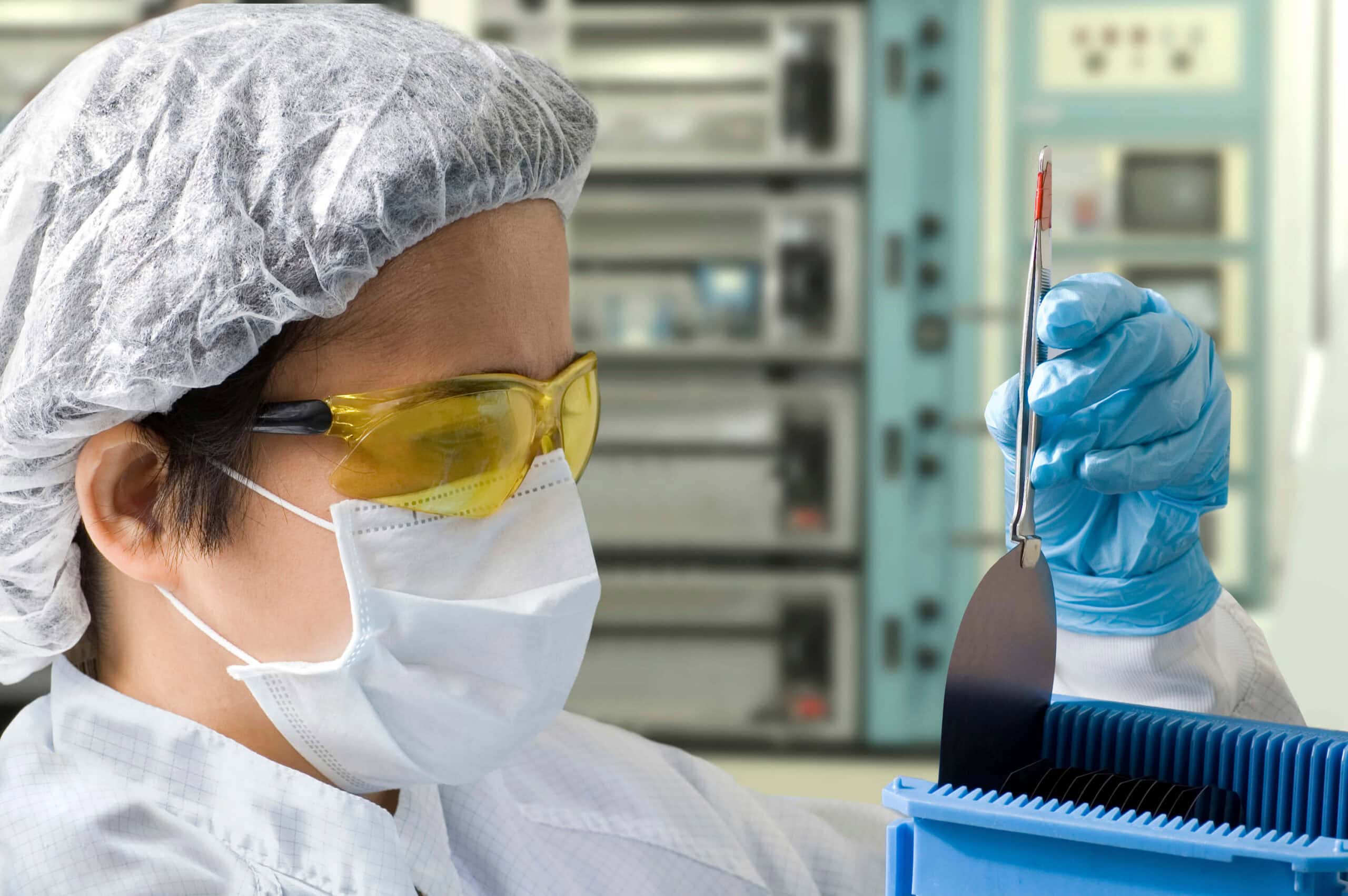
- Part handling of these ultra-thin wafers requires a deft hand and plenty of care. Although glass at this thickness does have some flexibility, there are limits to this. The previous two items also contribute to the level of flexibility and will impact how to handle the parts.
- Cleaning of ultra-thin wafers requires a significant amount of care to ensure that they do not break during this process.

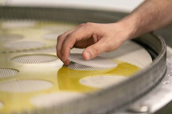
For single-side processing, we have processed wafers that have a valuable coating on the backside surface. By protecting this coating with a thin layer of photoresist, our experienced team of technicians can back-thin a standard wafer to 100 microns or even thinner.
For handling wafers in this process, blocking and deblocking techniques are critical to its survivability. The proper choice of wax is very important to ensuring that the bond is uniform, and any taper is minimized while also ensuring that the wafer remains attached to the blocking body throughout the entire manufacturing process.
LEARN MORE ABOUT OUR GLASS WAFER CAPABILITIES
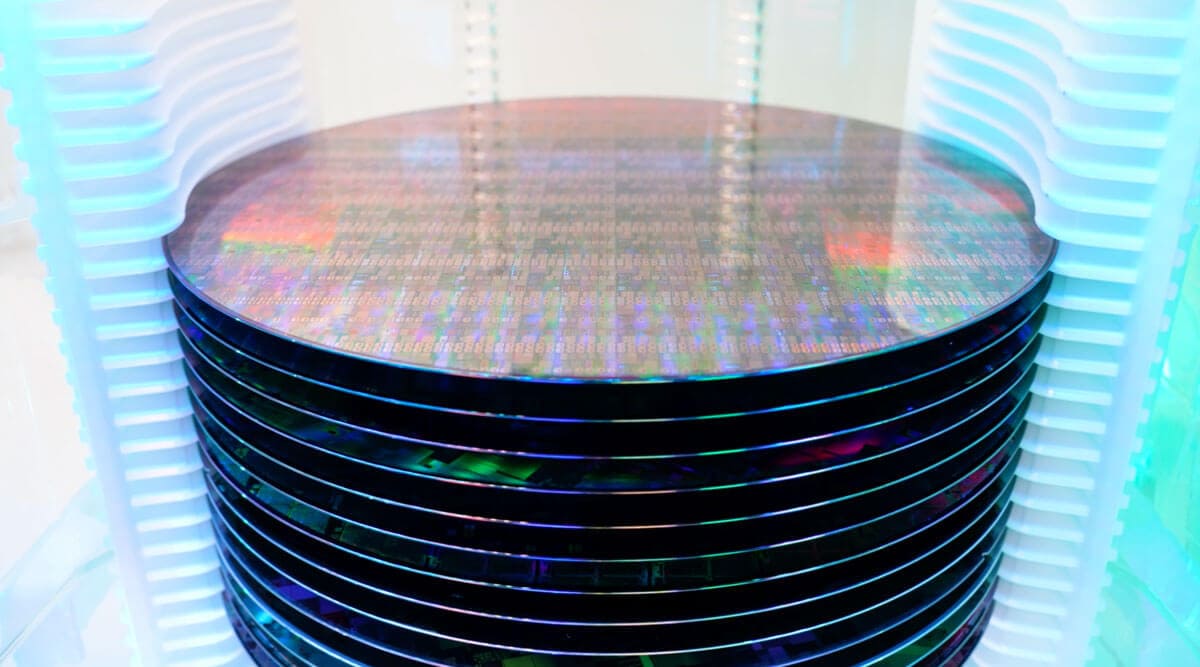
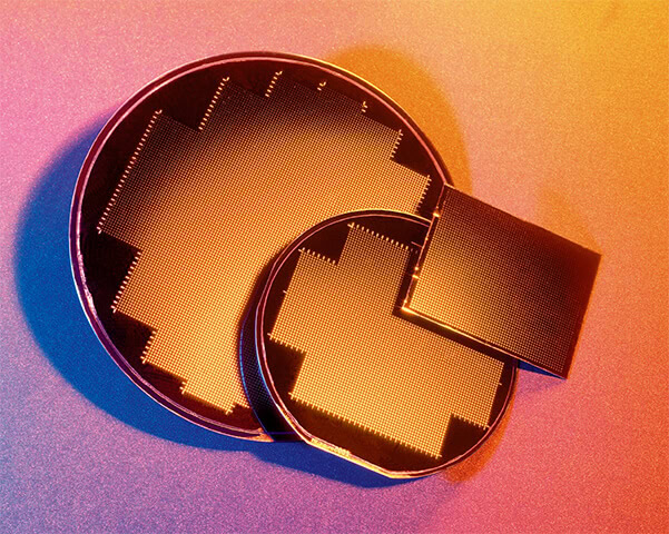
Aside from standard size glass wafers such as 100mm, 150mm, 200mm and 300mm, Sydor Optics can provide custom wafers with diameters up to 450mm and thin wafers with thicknesses down to 0.1mm.
ABOUT OUR EXPERIENCE IN GLASS WAFERS FOR SEMICONDUCTOR
Due to its properties and cost-effective solutions, glass substrates can be used as permanent or temporary materials in the semiconductor manufacturing process for chips and microchips in electronic devices. Wafers from Sydor Optics – for even ultra-thin semiconductor structures – are the ideal substrate for this application.
When it comes to double-sided grinding and polishing, we are the experts!
We consistently process parts 200 microns or thinner. There is a product line that we have been lapping/polishing for almost 20 years, with annual quantities generally ranging in the 20-60k pieces per year. The general advantages of double-side processing apply to thin parts in the same ways that they apply to thicker optics. Some accommodation will need to be made to ensure the stability of the tooling and the safety of the part while in the machine. Generally slower machine speeds and lower pressure are required to process thin parts.